Mechanically Controllable Break (MCB) junctions and Molecular Physics
During the last years there has been a substantial development in our understanding of tiny single molecule quantum systems. It turns out that the space, "nothing", embedding the system has a profound impact on the electrical characteristics of the system. By applying a microscopic layer of tetrahydrofuran (THF) fluid the embedding space can be electrically shielded from the system. The aim of this site is to provide insight in the fundamentals of these systems for everyone interested in this fascinating micro-world where new physics and quantum effects will be revealed.
Further reading:
- A pivoting mechanically controllable break junction setup enabling "partially wet phase" MCB-junctions. (arXiv 2021)
- Decoupling environmental modes from tunneling electrons in a partially wet phase molecular mechanically controllable break junction. (arXiv 2021)
- Detailing the natural creation process of a single molecule MCB junction in the partially wet phase. (arXiv 2021)
- The impact of a measurement on an open quantum system. (arXiv November 20 2024)
- Measuring the measurement problem: controlling decoherence with measurement duration in molecular MCB junctions. (arXiv October 2 2025)
A single molecule MCB junction in the partially wet phase
A quantum effect at ambient conditions is presented. A benzene dithiol (BDT) molecule or a tetrahydrofuran (THF) molecule is used as a barrier molecule bridging the gold electrodes from a Mechanically Controllable Break junction. It has been known for a long time that the environment of a junction couples to the conduction. With a microscopic layer of fluid it is actually possible to influence this coupling. The electrode-molecule-electrode configuration is lined with a microscopic layer of THF fluid, also known as the “partially wet phase”. This is effectively decoupling the electrode-molecule-electrode system from environmental modes outside of this system. The effects on coherence and quantum interference are exceptional.
An impression of a single molecule junction in the partially wet phase, not to scale. The blue/purple layer represents the THF partially wet phase layer. The red liner represents the finite width of the surface potential, trapping charge carriers at the THF/air interface. Thus, creating a miniature Faraday cage shielding the environment from the molecular system.
Decoupling environmental modes enabling one dimensional conduction
When technology enabled us to confine electrons to two dimensions an entirely new era in physics opened. Why did it take until the 80’s to get there? Electrons are small, in principle elementary particles such as electrons have a radius of zero! However, in solid state physics we can attribute a wave function to electrons which has a typical spatial extend of atomic dimensions. This implies that we need to build an atomically flat interface between two different materials. This will capture the electrons in a potential well shaped by the surface potential at the interface and form a two-dimensional electron gas (2DEG). Once people mastered this technique and started measuring on a 2DEG, the quantum Hall effect was discovered. A novel field emerged, for example by using gates isolated from, but near to, the 2DEG. New devices were created revealing novel physics.
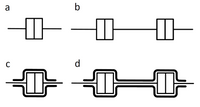
Schematic representatiaion of a: a single junction, b: a double junction, c: a single junction in the partially wet phase, d: a double junction in the partially wet phase.
What is the foremost issue that needs to be resolved to go from two to one dimension? It turns out to be something that most people would not expect. The space embedding the device is having an impact on the electrical behavior of the device. Even if this space consists of an absolute vacuum at zero temperature it does influence the device. Heisenberg teaches us that an absolute vacuum does not exist! It is possible to “borrow” energy from the vacuum for a small amount of time as long as there is pay-back according to Heisenberg’s relation:
The vacuum is full of photons and elementary particles which are short lived. Thus, there is a constant creation and annihilation of these “Heisenberg modes” or “vacuum environmental modes”.
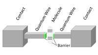
A schematic simplified representation of the junctions under study. The single molecule is connected to two quantum wires which are connected to bulk material, enabling true one-dimensional conduction.
Let’s create a one-dimensional device, one molecule connected to two leads of atomic dimension, called quantum wires, see the picture above. This device has a typical resistance in the 50 MΩ range. Conducting electrons will either be reflected by, or transmitted through, this structure. These electrons can interact with the Heisenberg modes from the embedded space and for example exchange energy. Due to this energy-exchange, we lose specific information. It turns out that if we shield the embedding space from the device with a Faraday cage, the interaction and thus energy-exchange between conduction electrons and Heisenberg modes in the embedded space is effectively blocked. A novel regime is opening.
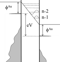
This figure shows the electronic equivalence of the image above. The one dimensional density of states peak of the quantum wires or equivalently, the atomic size electrodes, is ideally suited to probe mV resolution phenomena in solid state physics.


